Source: An Event-Driven E-Skin System with Dynamic Binary Scanning and real time SNN Classification
Authors: CityUHK
Goals: make a low power tactile skin for robotics
Notes.
the reasoning behind using SNNs for:
even with event driven scanning, systems still use ANNs for classification which causes a mismatch between the sparse event driven data and dense frames for ANN processing. also need too much compute / parameter counts for an embedded system.
Conv-SNN takes only 65% of the computation and 15.6% of the weight storage of a conventional CNN while having 92.11 classification accuracy. gives out heatmap of changes.
Hardware
hardware diagram of tactile system.
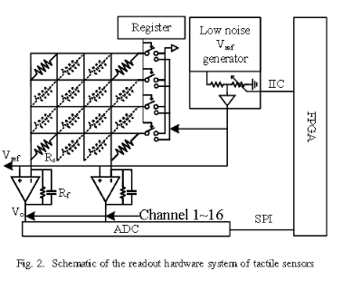
150mm x 150mm area of sensing, with 256 piezoresistive sensors (each measuring 7.5mm x 7.5mm).
piezoresistive sensors have resistance that decreases as applied pressure (susceptible to sharp objects showing malformed outputs) increases.
Vo = Vref (1 + Rf / Rs)
thoughts:
main benchmark is on handwritten digit recognition which is a bit weak.
uses FSRs only, so no multimodal sensing + also affected by “area” of touch instead of force.
Conversation with the Author
(1)We used a ZYNQ-7020-based development board to implement the control circuit for analog front-end data acquisition. This board allows digital logic circuits to be implemented through Verilog programming and provides a variety of external interfaces. Through these interfaces, we output digital signals to control our custom-designed PCB, thereby realizing an analog front-end acquisition system. The FPGA portion was implemented entirely in Verilog, without using the on-board CPU for embedded system design.
(2)The end-to-end latency is relatively difficult to calculate for this type of mixed digital–analog circuit. The digital logic implemented on the FPGA operates at a 50 MHz clock frequency. Under this clock, the ADC chip we used can theoretically sample the input signal at a rate of 781 kS/s. Since the sensor matrix has a size of 16 × 16, the theoretical upper limit is approximately 3,000 full-matrix samples per second. This represents the theoretical upper bound of the digital logic. However, the analog front-end circuit on the PCB in this work was not fully optimized to reach this limit. … In our current implementation, we achieved 200 full-matrix samples per second, which is already sufficient for our application. Regarding power consumption, we have not estimated or measured it.
(3)For the formula derivation, we assume that the matrix contains N elements, with only one point being activated. The algorithm then determines how many ADC scans are required to identify the activated point. … The expression contains two terms: one is a √N term, and the other is a log₂ term. The former corresponds to the channel-by-channel polling in the code, while the latter represents the time complexity required for binary scanning.
Best regards, Li Gaishan
In that paper, we ultimately trained the NN only on the PC side, while the FPGA was used solely to control data collection. Implementing a fixed NN on an FPGA mainly involves two approaches: a purely FPGA-based implementation and an embedded-system-based implementation. However, both approaches are not very flexible. The algorithm mentioned in the paper is indeed designed only for the single-point case; for the multi-point case, we plan to propose a new algorithm in combination with the hardware circuit design.